


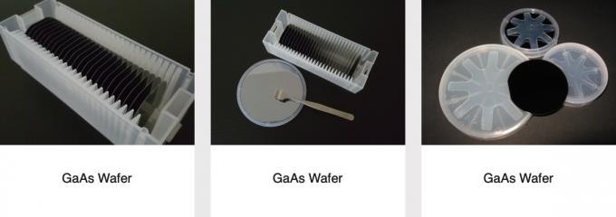
2 Inch 3 Inch 4 Inch Undoped Gallium Arsenide Wafer Semi Insulating GaAs Substrate For LED
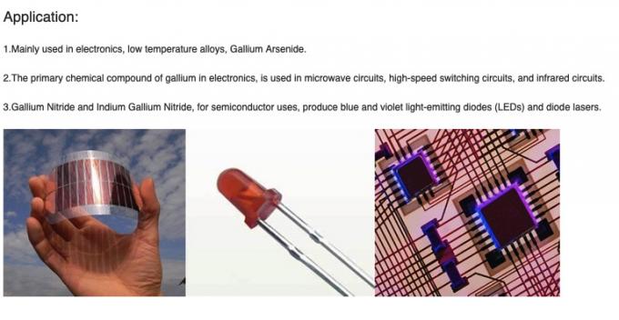
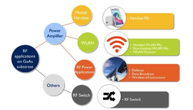
Feature Application field High electron mobility Light […]
Send Inquiry
Add To Cart
| Feature | Application field |
|---|---|
| High electron mobility | Light emitting diodes |
| High frequency | Laser diodes |
| High conversion efficiency | Photovoltaic devices |
| Low power consumption | High Electron Mobility Transistor |
| Direct band gap | Heterojunction Bipolar Transistor |
| Growth Method | VGF | ||
| Dopant | p-type: Zn | n-type: Si | |
| Wafer Shape | Round (dia: 2″, 3″, 4″, 6″) | ||
| Surface Orientation * | (100)±0.5° | ||
| * Other Orientations maybe available upon request | |||
| Dopant | Si (n-type) | Zn (p-type) | |
| Carrier Concentration (cm-3) | ( 0.8-4) × 1018 | ( 0.5-5) × 1019 | |
| Mobility (cm2/V.S.) | ( 1-2.5) × 103 | 50-120 | |
| Etch Pitch Density (cm2) | 100-5000 | 3,000-5,000 | |
| Wafer Diameter (mm) | 50.8±0.3 | 76.2±0.3 | 100±0.3 |
| Thickness (µm) | 350±25 | 625±25 | 625±25 |
| TTV [P/P] (µm) | ≤ 4 | ≤ 4 | ≤ 4 |
| TTV [P/E] (µm) | ≤ 10 | ≤ 10 | ≤ 10 |
| WARP (µm) | ≤ 10 | ≤ 10 | ≤ 10 |
| OF (mm) | 17±1 | 22±1 | 32.5±1 |
| OF / IF (mm) | 7±1 | 12±1 | 18±1 |
| Polish* | E/E, P/E, P/P | E/E, P/E, P/P | E/E, P/E, P/P |
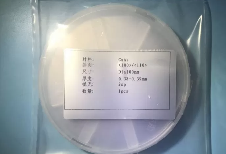
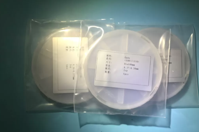
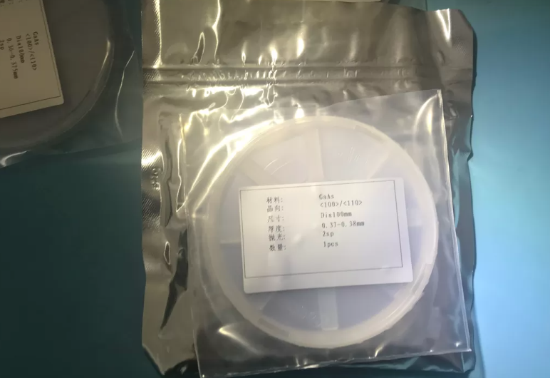
Specifications of semi-conducting GaAs wafer
Specifications of semi-insulating GaAs wafer
| Growth Method | VGF | |||
| Dopant | SI Type: Carbon | |||
| Wafer Shape | Round (DIA: 2″, 3″, 4″, 6″) | |||
| Surface Orientation * | (100)±0.5° | |||
| * Other Orientations maybe available upon request | ||||
| Resistivity (Ω.cm) | ≥ 1 × 10⁷ | ≥ 1 × 10⁸ | ||
| Mobility (cm2/V.S) | ≥ 5,000 | ≥ 4,000 | ||
| Etch Pitch Density (cm2) | 1,500-5,000 | 1,500-5,000 | ||
| Wafer Diameter (mm) | 50.8±0.3 | 76.2±0.3 | 100±0.3 | 150±0.3 |
| Thickness (µm) | 350±25 | 625±25 | 625±25 | 675±25 |
| TTV [P/P] (µm) | ≤ 4 | ≤ 4 | ≤ 4 | ≤ 4 |
| TTV [P/E] (µm) | ≤ 10 | ≤ 10 | ≤ 10 | ≤ 10 |
| WARP (µm) | ≤ 10 | ≤ 10 | ≤ 10 | ≤ 15 |
| OF (mm) | 17±1 | 22±1 | 32.5±1 | NOTCH |
| OF / IF (mm) | 7±1 | 12±1 | 18±1 | N/A |
| Polish* | E/E, P/E, P/P | E/E, P/E, P/P | E/E, P/E, P/P | E/E, P/E, P/P |
Send Inquiry
