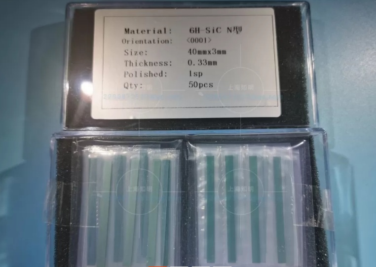
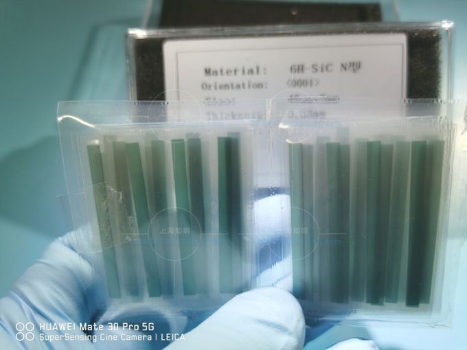
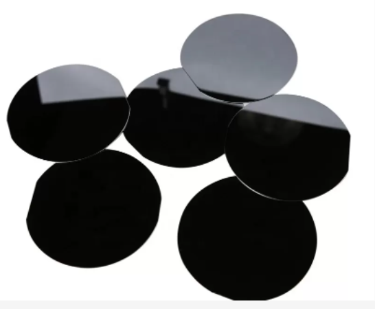
Optical Square 40x3mmt 6H-N Sic Silicon Carbon Chips
Silicon carbide (SiC), also known as carborundum, is a […]
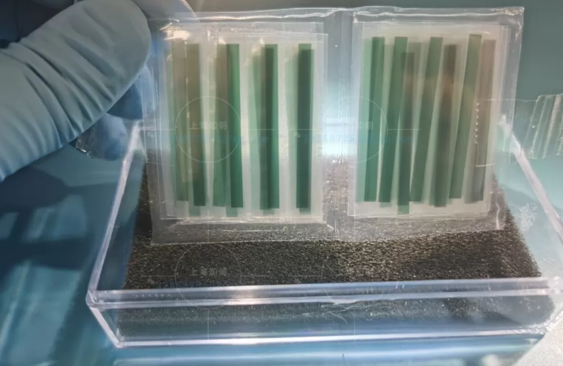
Silicon carbide (SiC), also known as carborundum, is a semiconductor containing silicon and carbon with chemical formula SiC. SiC is used in semiconductor electronics devices that operate at high temperatures or high voltages, or both.SiC is also one of the important LED components, it is a popular substrate for growing GaN devices, and it also serves as a heat spreader in high-power LEDs.
| Property | 4H-SiC, Single Crystal | 6H-SiC, Single Crystal |
| Lattice Parameters | a=3.076 Å c=10.053 Å | a=3.073 Å c=15.117 Å |
| Stacking Sequence | ABCB | ABCACB |
| Mohs Hardness | ≈9.2 | ≈9.2 |
| Density | 3.21 g/cm3 | 3.21 g/cm3 |
| Therm. Expansion Coefficient | 4-5×10⁻⁶/K | 4-5×10⁻⁶/K |
| Refraction Index @750nm | no = 2.61ne = 2.66 | no = 2.60ne = 2.65 |
| Dielectric Constant | c~9.66 | c~9.66 |
| Thermal Conductivity (N-type, 0.02 ohm.cm) | a~4.2 W/cm·K@298Kc~3.7 W/cm·K@298K | |
| Thermal Conductivity (Semi-insulating) | a~4.9 W/cm·K@298Kc~3.9 W/cm·K@298K | a~4.6 W/cm·K@298Kc~3.2 W/cm·K@298K |
| Band-gap | 3.23 eV | 3.02 eV |
| Break-Down Electrical Field | 3-5×10⁶V/cm | 3-5×10⁶V/cm |
| Saturation Drift Velocity | 2.0×10⁵m/s | 2.0×10⁵m/s |
Application of SiC in power device industry
| Properties | unit | Silicon | SiC | GaN |
| Bandgap width | eV | 1.12 | 3.26 | 3.41 |
| Breakdown field | MV/cm | 0.23 | 2.2 | 3.3 |
| Electron mobility | cm^2/Vs | 1400 | 950 | 1500 |
| Drift valocity | 10^7 cm/s | 1 | 2.7 | 2.5 |
| Thermal conductivity | W/cmK | 1.5 | 3.8 | 1.3 |
Compared with silicon devices, silicon carbide (SiC) power devices can effectively achieve high efficiency, miniaturization and light weight of power electronic systems. The energy loss of SiC power devices is only 50% of Si devices, and the heat generation is only 50% of silicon devices, SiC also has a higher current density. At the same power level, the volume of SiC power modules is significantly smaller than that of silicon power modules. Taking the intelligent power module IPM as an example, using SiC power devices, the module volume can be reduced to 1/3 to 2/3 of silicon power modules.
There are three types of SiC power diodes: Schottky diodes (SBD), PIN diodes and junction barrier controlled Schottky diodes (JBS). Because of the Schottky barrier, SBD has a lower junction barrier height, so SBD has the advantage of low forward voltage. The emergence of SiC SBD has enlarged the application range of SBD from 250V to 1200V. In addition, its characteristics at high temperature are good, the reverse leakage current not increases from room temperature to 175 ° C. In the application field of rectifiers above 3kV, SiC PiN and SiC JBS diodes have received much attention due to their higher breakdown voltage, faster switching speed, smaller size and lighter weight than silicon rectifiers.
SiC power MOSFET devices have ideal gate resistance, high-speed switching performance, low on-resistance, and high stability. It is the preferred device in the field of power devices below 300V. There are reports that a silicon carbide MOSFET with a blocking voltage of 10kV has been successfully developed. Researchers believe that SiC MOSFETs will occupy an advantageous position in the field of 3kV – 5kV.
SiC Insulated Gate Bipolar Transistors (SiC BJT, SiC IGBT) and SiC Thyristor (SiC Thyristor), SiC P-type IGBT devices with a blocking voltage of 12 kV have good forward current capability. Compared with Si bipolar transistors, SiC bipolar transistors have 20-50 times lower switching losses and lower turn-on voltage drop. SiC BJT is mainly divided into epitaxial emitter BJT and ion implantation emitter BJT, the typical current gain is between 10-50.
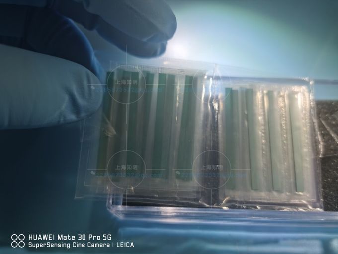
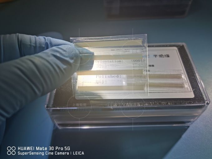

Silicon Carbide SiC crystal substrate wafer carborundum
The specification of 3” Inch
| Grade | Production | Research Grade | Dummy Grade |
| Diameter | 50.8 mm±0.38 mm or other size | ||
| Thickness | 330 μm±25μm | ||
| Wafer Orientation | On axis: <0001>±0.5° for 6H-N/4H-N/4H-SI/6H-SI Off axis : 4.0° toward1120 ±0.5° for 4H-N/4H-SI | ||
| Micropipe Density | ≤5 cm-2 | ≤15 cm-2 | ≤50 cm-2 |
| Resistivity | 4H-N | 0.015~0.028 Ω·cm | |
| 6H-N | 0.02~0.1 Ω·cm | ||
| 4/6H-SI | >1E5 Ω·cm | (90%) >1E5 Ω·cm | |
| Primary Flat | {10-10}±5.0° | ||
| Primary Flat Length | 22.2 mm±3.2 mm | ||
| Secondary Flat Length | 11.2mm±1.5 mm | ||
| Secondary Flat Orientation | Silicon face up: 90° CW. from Prime flat ±5.0° | ||
| Edge exclusion | 2 mm | ||
| TTV/Bow /Warp | ≤15μm /≤25μm /≤25μm | ||
| Roughness | Polish Ra≤1 nm | ||
| CMP Ra≤0.5 nm | |||
| Cracks by high intensity light | None | 1 allowed, ≤ 1mm | 1 allowed, ≤2 mm |
| Hex Plates by high intensity light | Cumulative area≤1 % | Cumulative area≤1 % | Cumulative area≤3 % |
| Polytype Areas by high intensity light | None | Cumulative area≤2 % | Cumulative area≤5 % |
| Scratches by high intensity light | 3 scratches to 1×wafer diameter cumulative length | 5 scratches to 1×wafer diameter cumulative length | 8 scratches to 1×wafer diameter cumulative length |
| Edge chip | None | 3 allowed, ≤0.5 mm each | 5 allowed, ≤1 mm each |
| Contamination by high intensity light | None |
SIC Silicon Carbide Wafer Quotation
Whatsapp +8618621835134
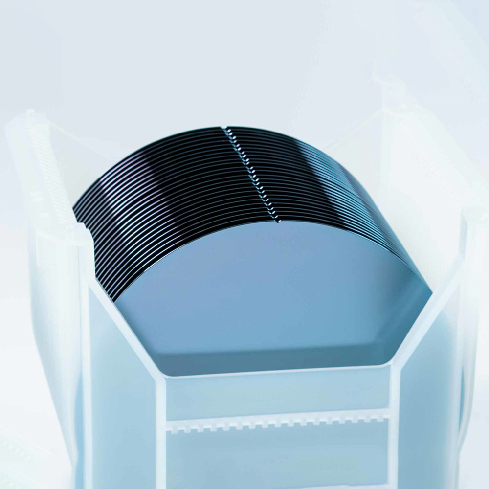
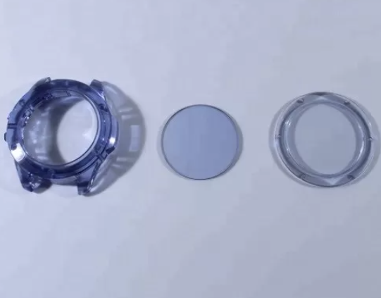
Send Inquiry

