

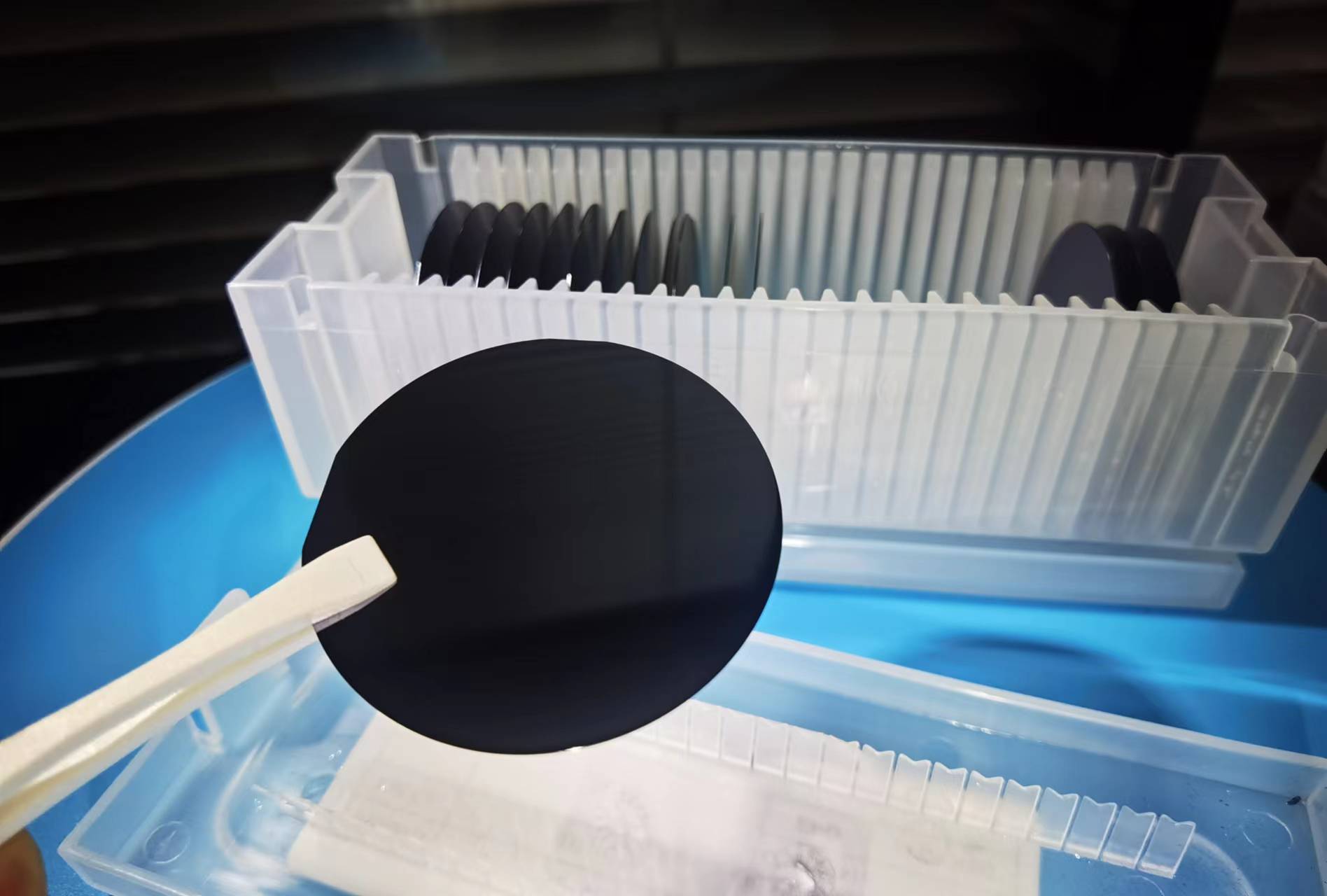
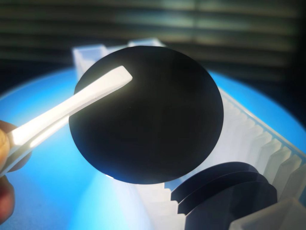
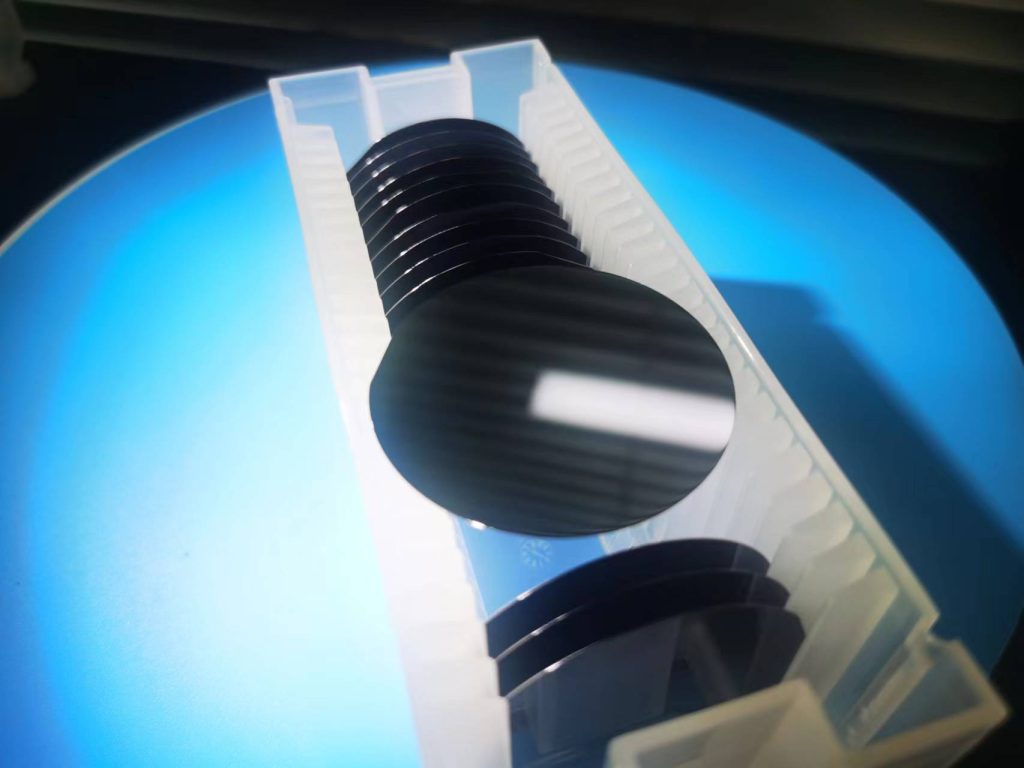
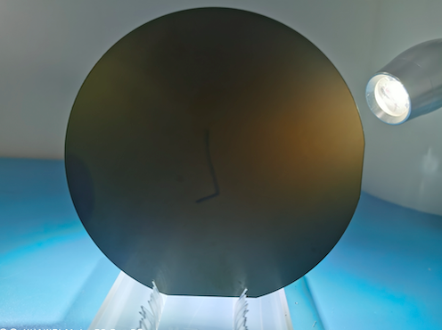
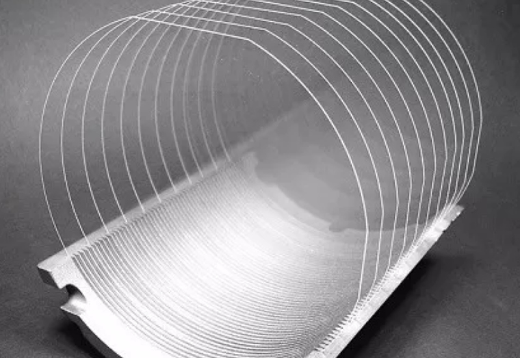
Gallium Arsenide (GaAs) Wafers for Research/Production
Growth Method VGF Dopant p-type: Zn n-type: Si Wafer Sh […]
| Growth Method | VGF | ||
| Dopant | p-type: Zn | n-type: Si | |
| Wafer Shape | Round (dia: 2″/3″/4″/6″) | ||
| Surface Orientation | (100)±0.5° | ||
| Other Orientations maybe available upon request | |||
| Dopant | Zn (p-type) | Si (n-type) | |
| Carrier Concentration (cm-3) | ( 0.5-5) × 1019 | ( 0.8-4) × 1018 | |
| Mobility (cm2/V.S.) | 50-120 | ( 1-2.5) × 103 | |
| Etch Pitch Density (cm2) | 3000-5000 | 100-5000 | |
| Wafer Diameter (mm) | 76.2±0.3 | 100±0.3 | 50.8±0.3 |
| Thickness (µm) | 625±25 | 625±25 | 350±25 |
| TTV [P/P] (µm) | ≤ 4 | ≤ 4 | ≤ 4 |
| TTV [P/E] (µm) | ≤ 10 | ≤ 10 | ≤ 10 |
| WARP (µm) | ≤ 10 | ≤ 10 | ≤ 10 |
| OF (mm) | 22±1 | 32.5±1 | 17±1 |
| OF/IF (mm) | 12±1 | 18±1 | 7±1 |
| Polish | E/E | ||
| P/E | |||
| P/P |
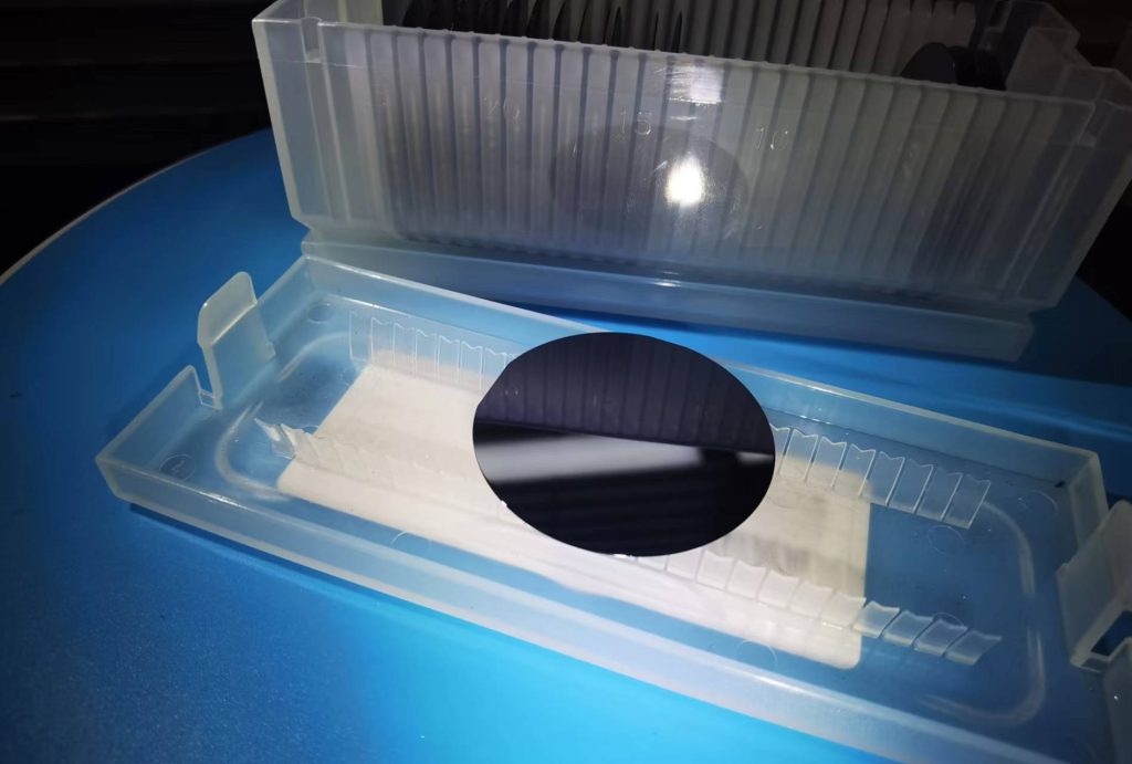
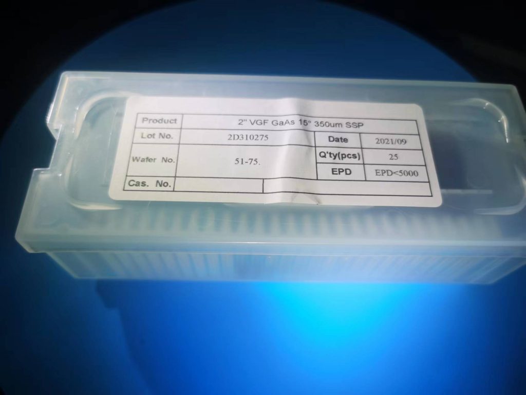
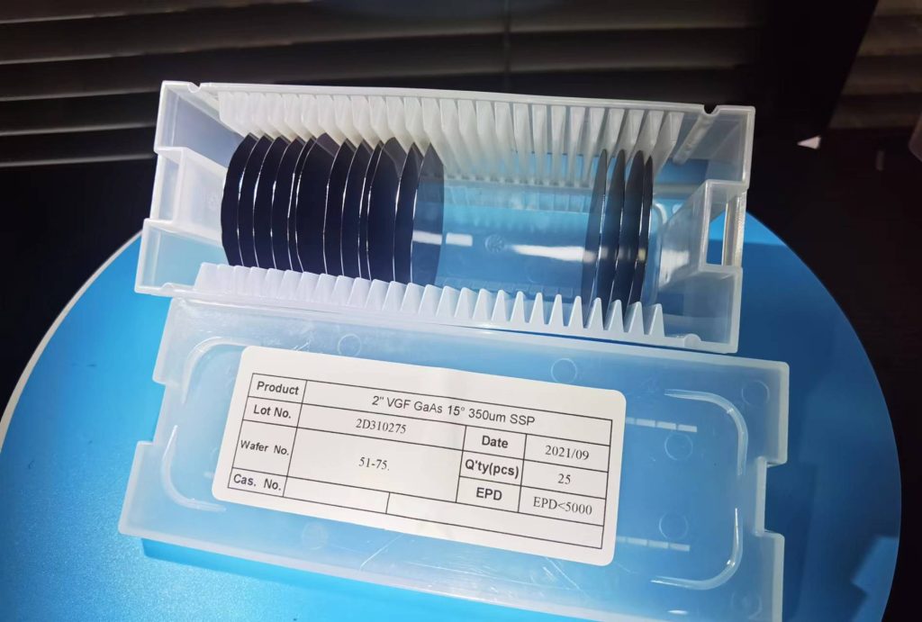
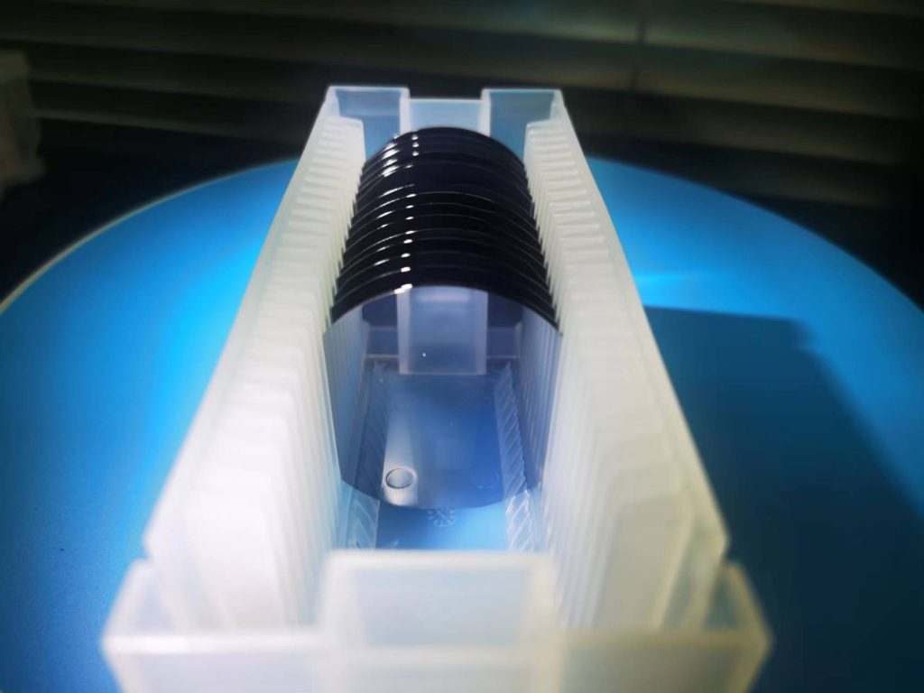
Gallium Arsenide (GaAs) Wafers Package
Application of Gallium Arsenide (GaAs) Wafers
High electron mobility
High frequency
High conversion efficiency
Low power consumption
Direct band gap
Light emitting diodes
Laser diodes
High Electron Mobility TransistorPhotovoltaic devices
Heterojunction Bipolar Transistor
Gallium Arsenide (GaAs) Wafers
related semiconductor wafers
FAQ
A)Does the product have standard specifications?
Our factory needs you to provide drawings or samples for customized processing.
B)Can I get some samples?
Yes, please purchase samples directly online, or send drawings to us for us to make.
C)What’s the delivery time?
The production cycle of the product is about 45 days, and the transportation time is 4-5 days,
depending on the distance, the transportation mode will affect. Would you please understanding.
D)How do you guarantee the quality of your products?
We have strict inspection standards. It will be inspected again before
packing.
E)How do you guarantee the quality of your products and how do you deal with quality problems?
Our products are produced under strict quality control system.If the quality problem is caused by our factory, we provide warranty service. For batches with problems, we will discuss solutions, including recalls, based on the actual situation.
Send Inquiry
