

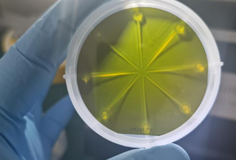
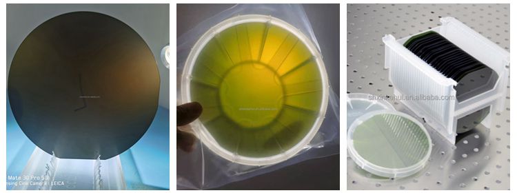
Polished 100mm SIC Epitaxial Silicon Carbide Wafer 1mm Thickness For Ingot Growth
Description of Sic Wafer Property 4H-SiC, Single Crysta […]
Send Inquiry
Add To Cart
Description of Sic Wafer
| Property | 4H-SiC, Single Crystal | 6H-SiC, Single Crystal |
| Lattice Parameters | a=3.076 Å c=10.053 Å | a=3.073 Å c=15.117 Å |
| Stacking Sequence | ABCB | ABCACB |
| Mohs Hardness | ≈9.2 | ≈9.2 |
| Density | 3.21 g/cm3 | 3.21 g/cm3 |
| Therm. Expansion Coefficient | 4-5×10⁻⁶/K | 4-5×10⁻⁶/K |
| Refraction Index @750nm | no = 2.61 ne = 2.66 | no = 2.60 ne = 2.65 |
| Dielectric Constant | c~9.66 | c~9.66 |
| Thermal Conductivity (N-type, 0.02 ohm.cm) | a~4.2 W/cm·K@298K c~3.7 W/cm·K@298K | |
| Thermal Conductivity (Semi-insulating) | a~4.9 W/cm·K@298K c~3.9 W/cm·K@298K | a~4.6 W/cm·K@298K c~3.2 W/cm·K@298K |
| Band-gap | 3.23 eV | 3.02 eV |
| Break-Down Electrical Field | 3-5×10⁶V/cm | 3-5×10⁶V/cm |
| Saturation Drift Velocity | 2.0×10⁵m/s | 2.0×10⁵m/s |
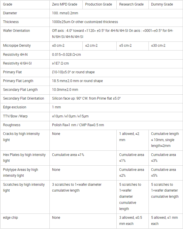
4H-N 4inch diameter Silicon Carbide (SiC) Substrate Specification
Silicon carbide (SiC), also known as carborundum, is a semiconductor containing silicon and carbon with chemical formula SiC. SiC is used in semiconductor electronics devices that operate at high temperatures or high voltages, or both.SiC is also one of the important LED components, it is a popular substrate for growing GaN devices, and it also serves as a heat spreader in high-power LEDs.
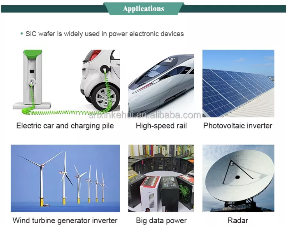
SiC Wafer Applications
- 1 high frequency and high power electronic devices Schottky diodes, JFET, BJT, PiN,
- diodes, IGBT, MOSFET
- 2 optoelectronic devices: mainly used in GaN/SiC blue LED substrate material (GaN/SiC) LED
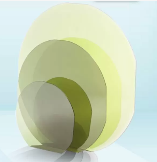
CATALOG COMMON SIZE In OUR INVENTORY LIST
| 4H-N Type / High Purity SiC wafer/ingots2 inch 4H N-Type SiC wafer/ingots 3 inch 4H N-Type SiC wafer 4 inch 4H N-Type SiC wafer/ingots 6 inch 4H N-Type SiC wafer/ingots | 4H Semi-insulating / High Purity SiC wafer2 inch 4H Semi-insulating SiC wafer 3 inch 4H Semi-insulating SiC wafer 4 inch 4H Semi-insulating SiC wafer 6 inch 4H Semi-insulating SiC wafer |
| 6H N-Type SiC wafer 2 inch 6H N-Type SiC wafer/ingot | Customzied size for 2-6inch |
Send Inquiry
