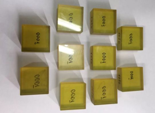
Single Crystal Superconducting Thin Monocrystalline Substrate 10X10mm Orientation Zinc
Product Name: Zinc oxide (ZnO) crystal substrate P […]
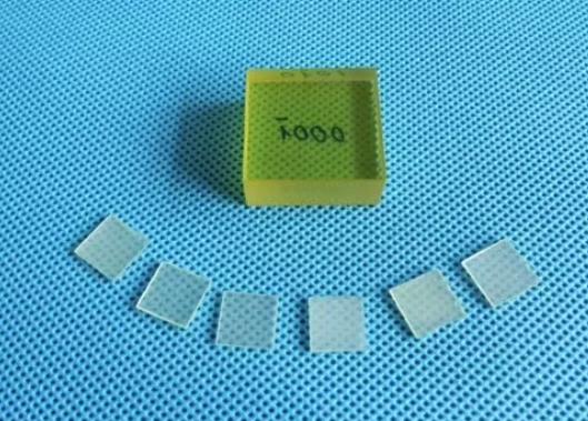
Product Name: Zinc oxide (ZnO) crystal substrate
Product Description: Zinc oxide (ZnO) crystal substrate is widely used in GaN (blue LED) epitaxial substrate, broad band connecting devices and other fields.
Technical parameters:
| Crystal structure | Hexagonal; a = 3.325 Åc = 5.213Å |
| Melting point (°C) | 1975 |
| Density (g / cm 3) | 5.605 |
| Heat capacity (J / gk) | 0.125 |
| Coefficient of thermal expansion (10 -6 / K) | 6.5 / / a; 3.7 / / c |
| Thermal conductivity (W / m.kat 300K) | 30 |
| Transmission wavelength (μm) | 0.4 ~ 0.6 |
| Index of refraction | 1.922 (o); 1.936 (e) |
Specifications: Growth method: hydrothermal method; Maximum size: 20x20x10mm; Note: You can also customize according to customer demand special orientation and size.
Standard Packaging: 1000 clean room, 100 clean bag or single box packaging
Application of Superconducting Thin Monocrystalline Substrate
ZnO material is a wide bandgap semiconductor material with direct band gap. It is a multifunctional crystal with luminescent, electro-optic, scintillation, semiconductor and other properties. It is an excellent key material for ZnO, GaN epitaxial films and devices. Short-wavelength light-emitting devices such as LEDs and LDs have great potential for development, and have become another research hotspot in the field of wide-bandgap semiconductors after GaN.
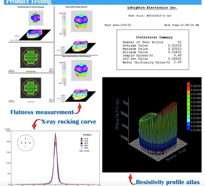

FAQ
Q. Do you have any stock of wafer or ingots?
yes,aslike 3inch,4inch commen size substrates wafers are in stocks.
Q. Where is your company located?
Our company located in shanghai,China. factory is in wuxi city.
Q. How long will take to get the products?
Generally it will take 1~4 weeks to process and then delivery.
It is depend on the quantity and the size of the products.
Q: How about pay term & delivery ?
T/T 50%deposit and left part before delivery by FOB .
Send Inquiry

